
CDLF-type 0805 Size Differential Chip Delay Line
- Smaller & lower cost than our existing products
- 10ps increments
- 15GHz Band width, available for 10Gbps data signals
- Suitable for inter-lane de-skew on multi-lane high speed serial transmission
- Solves the problems of space usage and the characteristic degradation of the substrate trace.(Please See Technical Note)
- Production: Now
- Based on your requirements, 0805 size single-ended Delay Lines are also possible.
Specifications

Package Dimensions and Pin Configuration

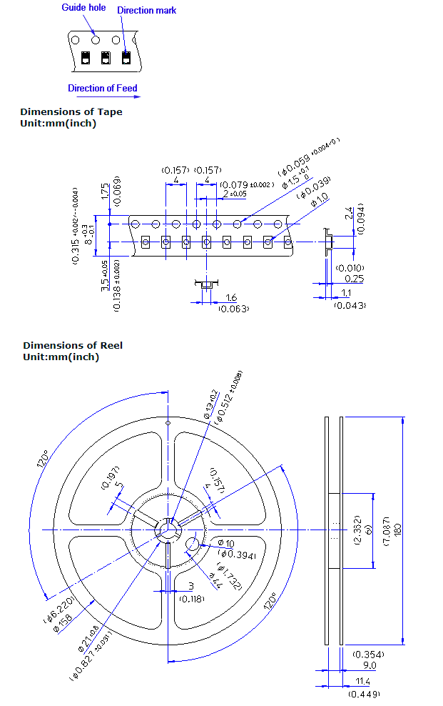
CDLF-Type Tape and Reel specifications
Shown below are the packing and product arrangement details for 3000-pc Tape & Reel. Please note, T&R MOQ is 500 pcs with 500-pc increment increases. Packing is embossed carrier tape with attached cover tape. The ELMEC Part Number, Lot Number, Quantity and RoHS-compliance (RoHS=Y) are shown on the reel surface.
Suggested Land Pattern

Reflow Soldering Conditions

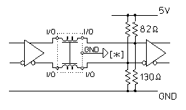
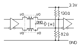
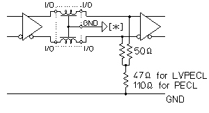
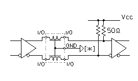
Typical Applications and Termination Methods
(1) PECL
(2) LVPECL
(3) Twisted Pair Termination
(4) LVDS

(5) CML
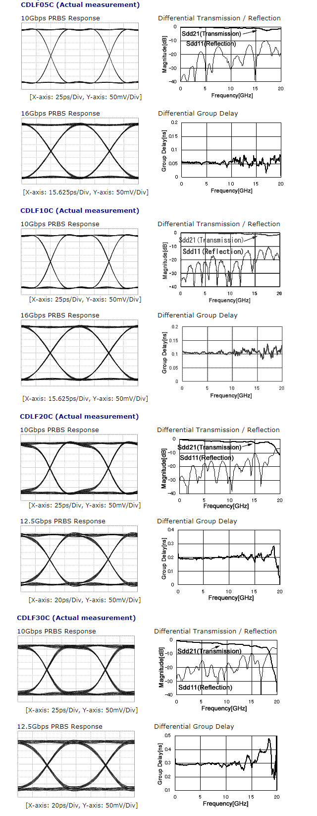
Output Waveforms - CDLF05C (Actual measurement)
Technical Note
Within tens of picoseconds of delay time adjustment, a substrate trace can be used for the return circuit. For a 100ps adjustment, either a substrate trace of a coupled differential pair, as shown in Fig.1, or a substrate trace of an uncoupled differential pair, as shown in Fig.2 can be assumed. However, the trace area in either case will become very large. Moreover, as shown in Fig. 1, a time lag arises between the differential pairs due to the imbalance at the corner. Common mode noise will occur at the mid-point, as will the fear of noise radiation. It is very likely that high-quality 10GHz+ band width characteristics cannot be obtained for the circuit shown in Fig.2. Fig.1 and Fig.2 are verified with an electromagnetic simulator and the characteristics are compared to the results utilizing the CDLF10C. The published Recommended Land Pattern is assumed for the substrate: W=0.38mm, t=0.3mm, and εr=4.1. The underside of the substrate is GND plane.
